You are here
Thick porous boron-doped diamond layers
Garant:
V. Mortet
Description:
The controlled enlargement of the specific surface area is an important enhancement of electrochemical electrodes. The Institute of Physics C.A.S. has developed a new patented process that allows the fabrication of thick porous boron-doped diamond (several 10s of micrometers) over large area (up to 200 x 300 mm2) for electroanalysis or water treatment.
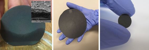
Figure: (left) 1.5-inch silicon wafer coated with a thick porous boron-doped nanocrystalline MWPECVD diamond layer (inset: cross-section SEM picture of porous boron-doped diamond); (middle) 4-inch silicon wafer coated with a thick porous boron-doped nanocrystalline MWPECVD diamond layer; (right) Æ 10 mm freestanding porous boron-doped nanocrystalline MWPECVD diamond disk.
Copyright © 2015 OFM AV ČR, v. v. i.